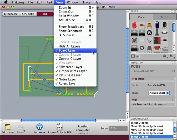
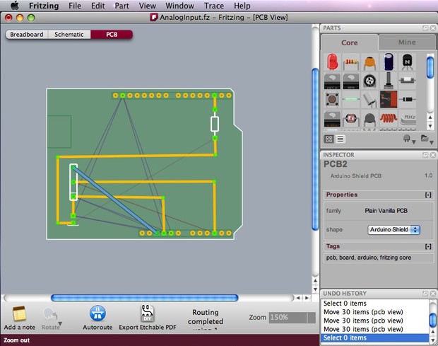
Fritzing's View options in the menu bar let you choose between different layers that can be shown or hidden to your convenience. In PCB View, some of these layers might be unfamiliar if you're new to PCB design. Lets go through them and make things clearer. 
- Board Layer - shows the board on which the circuit will be printed. In the example below - an Arduino shield. (DARK GREEN)
- Copper Layer - the copper traces are the actual soldering points and connections between parts. (ORANGE/LIGHT GREEN)
- Silkscreen Layer - Line art and text may be printed onto the outer surfaces of a PCB by silkscreen printing. Silkscreen print text can indicate component outline and designators, switch setting requirements, test points, and other features helpful in assembling, testing, and servicing the circuit board. (WHITE)
- Jumper wires Layer - acts as a guideline and shows connections that will need to be soldered with external wires after production.(BLUE)
- Rat's nest Layer - acts as a guideline and shows all the existing connections in the circuit. It is especially important to take into account while hand-routing. (shown as narrow connecting lines, each nest has its own color)
