Etching is a "subtractive" method used for the production of printed circuit boards: acid is used to remove unwanted copper from a prefabricated laminate. This is done by applying a temporary mask that protects parts of the laminate from the acid and leaves the desired copper layer untouched.
You can etch a PCB by yourself, in a lab or even at home, through a simple and inexpensive production process. It makes sense when you wish to produce a single or a very small number of boards and want to avoid manufacturing costs. The etching process is therefore effective for a small workshop. There are however some issues to consider:
- There is a risk of injuries due to the chemicals involved.
- The quality of the results depends on several factors which you won't be able to master completely the first time. This can be somewhat compensated by using good machinery.
- There is the problem of waste disposal. Toxic chemicals require a proper disposal service.
To learn how to etch a PCB, make sure that your Fritzing PCB design is complete and exported as an etchable PDF or SVG, then follow these instructions.
Safety
Since the work involves dangerous chemicals and power tools - you will need to take the necessary safety precautions:
- Wear safety equipment during the whole process - gloves, protection glasses, and an apron
- Work near an emergency eyewash station, a first aid box and a phone
- Familiarize yourself with the proper use of all equipment and tools in the lab - if you are unsure of anything, ask a member of the lab staff
Masking
There are different ways to produce a mask. We describe two simple methods:
Method A: Direct Toner Transfer
The circuit layout is printed with a laser printer on paper, put face-down on the laminate, and the toner is transfered from the paper to the copper using an iron.
Note that not every paper is suited for this method, including the standard printer paper, but a lot of success stories tell about reused magazin pages. Especially the Reichelt electronic catalogue should produce good results...
The print must be of a very good quality, little mistakes we usually tend to ignore in printed text can result in unusable traces or even cause short circuits. The transfer of the toner is a bit tricky as well. If temperature is too high, the toner gets too liquid and the tracks will blur. If the temperature is too low, the toner won't stick to the copper. After the ironing you can't pull the paper away just like that, without destroying half of the mask. Instead you have to put the laminate with the paper in a water bath and wait a while until you can start to cautiously scrub away the paper. This may take up to half an hour. You might want to check out this tutorial.
Method B: Photo-resistive laminates (Recommended)
The mask is printed on a transparent paper or foil, exposed and developed on the laminate with a UV lamp.
The laminates have a coating that is sensitive to light - by shining a light on them, we can transfer an image of the design to be created onto the board. Where light strikes the board, the coating weakens and creates an area of copper that will be dissolved away by the etching acid.
You will need a UV imaging frame and a photo development kit. Follow these steps:
- Export your PCB layout from Fritzing using File > Export > Etchable PDF/SVG. If you like, you can now edit and enhance the graphics in a graphics software.
- Print the file in highest resolution, first on white paper, and when satisfied, on a transparent paper or foil. Be careful to set the printer options to NOT "scale to fit".
- When printing on foil, use either a special toner or a toner dissolver spray to heighten the density and get the print tone overall even.
The spray should be used directly after printing, and care should be taken not to cause any drops. After the toner dries, place the foil in the imaging frame, toner side up. - Peel the protective blue film off the laminate and place it in the imaging frame copper side down, on top of the transparent film. Make sure not to expose the light-sensitive layer to too much light during the development process.
- Close the lid of the imaging frame, set the timer for 4 minutes and press the knob to start the exposure.
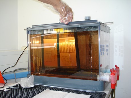
- Once the imaging process finishes, place the board in the development tank for 1-2 minutes and shake it once in a while (be careful not to leave it too long, otherwise it will damage the traces).
- Place the board in the rinse tank containing destillated water for a few seconds.
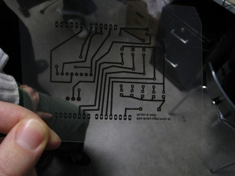
Printed mask on a foil
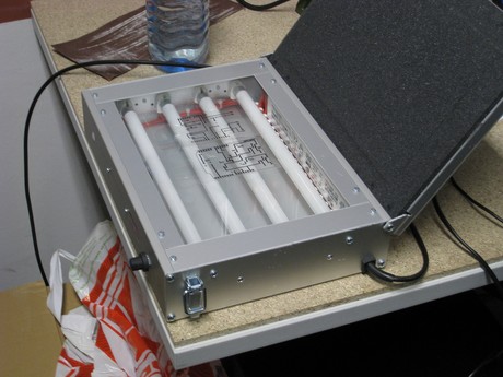
Placing the mask in the UV imaging frame
We recommend the photo-resistive laminates method even though it is a bit more expensive, because you only need to make a good mask template once and the imaging process should produce constantly good results on the laminates. The direct toner transfer on the other hand destroys the used template during transfer and while this is no problem for the production of a single PCB it will be a lot of hassle for multiples.
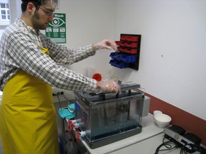
Etching
Different machines and chemicals can be used for etching, which will affect the comfort, duration and quality of the result.
Two Acid types that can be used for etching are ferric chloride (Eisen-3-Chlorid) and Sodium Persulfate (Natriumpersulfat - Feinätzkristall).
Although etching can also be done in simple plastic boxes, the quality of the results will improve dramatically when using a machine that controls temperature and constantly keeps the fluids in motion. There are small etching tanks with heating and air pump and there are small spray etching machines which can handle bigger PCBs and even the development and cleaning processes involved. The sprayer also decreases the etching time and the amount of acid needed.
To get rid of all unwanted copper follow these etching steps:
- Put the board in the acid tank for about 20 minutes until the copper traces are completely etched. You can tell that it's finished when the board turns from opaque pink to transparent yellow.
- Move the board into the rinse tank for a few seconds. You can also use an Isopropanol spray.
- Dry the board with a cloth.
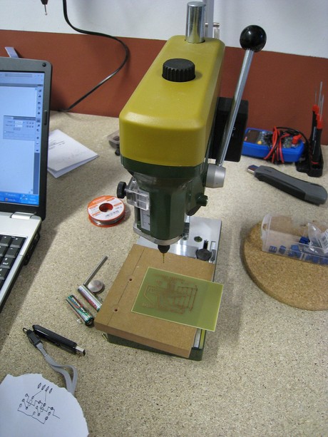
Drilling
To complete the PCB production, fix the board to a piece of wood, drill holes (holes should be at least 0.1 mm bigger than pins/wires), and cut the board to the desired size. You can also use varnish spray as a finishing coat.
Congratulation! Your PCB is ready!
There is actually a lot more you can learn about PCB production, but we hope this tutorial is a good starting point. You can also download the more detailed
"Introduction for working in the PCB lab of the FH Potsdam"
(in German) or read this useful tutorial.
Please feel free to contact us if you have any questions or tips.