ESP01 development board

A simple board to flash and operate the ESP01 board


A DIY development board for the ESP01
What is this?
A simple board useful to develop and test projects using the ESP01, a tiny board hosting an 8266, an MCU with an integrated WiFi network interface.
The assembly requires some experience with soldering, and the cost of the project is around 20$.
Once you have cloned the repository, open the .fzz file to see the board and understand the description below.
What is this for?
If you come from Arduino, the first experiences with the ESP01 (and other similar WiFi-able MCUs) are frustrating for two main reasons:
- the switch from Upload to Operate is not fully automatic;
- the operation of the board needs a regulated voltage of 3.3V;
- the operation of the WiFi device drains a relevant power.
I designed this elementary board to help the hobbist willing to try the ESP01 device and its builtin WiFi interface. I also assume that you are interested in reprogramming the device, not simply to use the AT style API that is pre-installed in the device.
There are a number of guides in the Internet that teach how to flash custom software in the ESP01, so I consider that you have already managed to play with a led on the GPIO2 pin. But you probably had problems to use the WiFi interface. The name of the problem is rst cause:4, boot mode:(3,7). If you understand me, you are ready to proceed...
Design overview
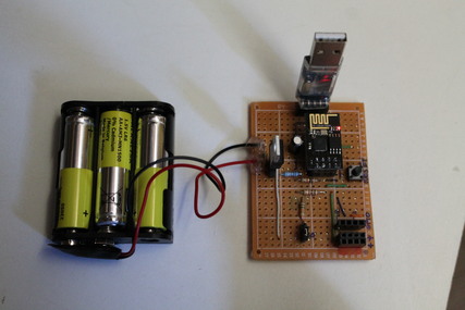
The development board is connected to your PC (hosting the Arduino IDE that is used to compile and flash the software) with a USB-TTL/USB-STC-ISP adapter that needs to be bought separately (less than 10$ on Internet shops). As a matter of fact the 3.3V output from my adapter is not powerful enough to drive the ESP01 WiFi interface, so I added an external power and a regulator.
The development board has a connector for the ESP01 board. There are also connectors that simplify the utilization of the data pins of the ESP01.
An LM317T IC stabilizes an external power source, like a 9V battery or a pack of 3x1.5V batteries.
A jumper helps to change from Upload to Usage mode and back with minimal effort.
A button resets the ESP01 device: this is needed to effect the mode switch.
The components are soldered on a 5x7cm perfboard: we have 8 connectors, one capacitor, four resistors, one button, one battery, and one integrated circuit LM317T.
Using the given values for the resistors, you will power the ESP01 with slightly more than 3.3, namely 3.6. As seen in the data sheet, this should not damage the device, but if you want exactly 3.3 you can modify the circuit adding a variable 500 Ohm resistor trimmer in series to R4.
CAUTION: USB-TTL/USB-STC-ISP adapters may have different pinout: the one I used in the design is (only bold ones are used):
3.3V - 5V - **TXD - RXD - GND**
You may need to change the connection of the J6 connector.
Operation
Preliminary setup
- plug the ESP01 MCU in the middle 8-pins connector (J4-J5)
- plug the USB-TTL/USB-STC-ISP adapter into the J6 connector
- short the two left pins of the J7 connector with a jumper
- connect at least 3x1.5V battery (a 9V battery is fine as well)
- push the reset button
- plug the adapter into a USB socket in your PC
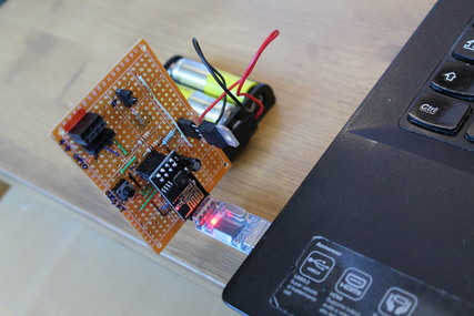
Now you are in Upload mode, ready to upload your sketch: I assume that you know how to do that.
When the upload is over, switch to the Usage mode in order to see it running:
- unplug the USB-TTL/USB-STC-ISP adapter from the J6 connector
- remove the jumper
- press the reset button
To flash again:
- plug the USB-TTL/USB-STC-ISP adapter into the J6 connector
- short again the J7 pins
- push the reset button
and you are ready to flash again!
Expansion connectors
The three connectors J1, J2 and J3 are used to connect the D0-3 pins and the power to a breadboard or such. J1 is for the 3.3 volts power, J2 for the ground, J3 for the data pins. The four pins are connected in the following order
D0 - D1 - D3 - D2
D2 being the most external.
Remind
The ESP01 has 4 data pins available, but three of them have a role while uploading: one (GPIO0) is used at boot, another two are used for communication during bootloading. Only one is permanently available, GPIO2. If you plan to use also the others for your experiments, keep in mind that your external equipment must not interfere with RX/TX during bootload, and that GPIO0 must be HIGH at boot time, but it can change state afterwards. In short, disconnect external devices connected to D0, D1 and D3 during the upload.
Testing
Before plugging the ESP01 in the development board, power the board and check that the polarity of the power pins is correct, and that the connections are as expected. Disconnect the power and connect your ESP01 and the USB adapter. Power the board and check that the leds on both devices are on. Now you can proceed with the sketch I used for testing: https://github.com/AugustoCiuffoletti/ESP01-TS-DHT11. Instead of the output from the DHT device you can provide random data.