Making a professional PCB has long been a task recommended for professional engineers and hardcore nerds only. The major goal of Fritzing is to lower this barrier to entry. While our software has made designing circuits much easier, producing an industry grade PCB was still tough without understanding a lot of specialized tools and jargon, UNITIL NOW! Fritzing proudly presents our new simple PCB fabrication service that takes your sketch and turns it into a working, professionally manufactured (and quite nice looking) circuit board. Here's how it's done:
1. DESIGN YOUR BOARD
Other areas of this site cover getting started with Fritzing, designing a circuit and laying out the PCB. If you want to do fancy stuff check out the tutorials on how to make your own custom parts and custom PCB shapes.
2. PREPARE YOUR BOARD FOR PRODUCTION
If you are new to production or not sure about things here are a few extra steps that you can follow in order to make sure you get the result you expect. Experienced fab folks can skip straight to step 3. Upload to the Fab.
A. OPTIMIZING
Even if you are not planning to produce 10,000 boards there are a few things you can do to make sure your design is reasonably efficient.
First, you need to make sure that the traces are the right dimensions for your design. A good rule to follow is that shorter, thicker traces are better than longer, thinner traces.

Next clean up funky routing. The Fritzing autorouter is not always the smartest and sometimes it ends up drawing wild traces that jump around the board. These can usually be tidied up by deleting bend points or moving some of them around. Shift-dragging bend points with the mouse will help make nice clean angles.
Finally, take a look at the board dimensions. The price you will pay is based on the total area of the board, so if you can nudge some parts and traces into a smaller rectangle, you can save some cash. Often just moving parts a few millimeters can pack things in more economically, but don't go crazy trying to be perfect. Also, don't forget to consider the mechanical fit. If you plan to squeeze your board into an Altoids tin or a pill box, you will need to make sure that it's the right size and shape. The ruler part (in the core bin at the bottom) can be a big help here. Keep it tight but make sure to have a little bit of space around the edges of the board.
B. CHECK FOR PROBLEMS
Even the best designers make mistakes so it's really important to check for some obvious errors.
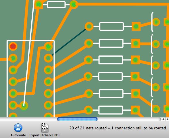
To begin with, make sure all the traces have been routed. The main window in the PCB view should say "Routing completed" at the bottom. If it says there are still connections to be routed, go find the colored rat's nest lines on the board and put in the missing traces.
Then, run the Design Rules Check (DRC) under the trace menu. The DRC will try to find mistakes that will break your circuit: shorts, overlaps, silk on the pads, things falling off the board, etc. Step through and fix each of these until your DRC passes.
Next, make sure your high-power connections are thick enough. Connections to motors, relays, batteries, lamps, big LEDs and other high power parts typically pull a lot more current. These connections need to to have "thick" or "extra thick" traces. Use "thick" traces for anything over 500mA and "extra thick" for 1.5A and up. You can change trace thickness by selecting the trace and modifying the "width" parameter in the Inspector. When in doubt it's always safe to use fatter traces as long as you have enough room.
Finally, don't forget to run "Copper Fill" under the "Trace" menu. This fills in the blank areas of your PCB with copper. This helps make your board a bit more resilient to electromagnetic interference and produces less nasty chemical waste since there's less to etch away. It also looks a bit sexier.
C. DOES IT LOOK RIGHT?
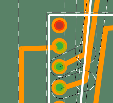
Now, after optimizing and verifying your design, take a good long human look at it and make sure that the connections are all correct and that there's nothing missing. There's nothing more frustrating than soldering your board together only to realize that you forgot one connection. It's often useful to print out your sketch (File->Print) and sit down with a pencil and step through all the connections in multiple views, just to confirm there are no little mess-ups.
[PARTS ON PAPER PHOTO]
If you have your parts, you can also use the PDF printout as a sort of paper placement test. Just put your parts on the paper in the places where they belong. They should fit almost exactly as long as you disabled any scaling options in the Print dialog. You may find that one or two have footprints that are too big, too small or just plain wrong. In that case, you should adjust the Fritzing part or substitute for one with the appropriate dimensions.
D. PROOF YOUR PRODUCTION FILES
This last check is optional but it often helps to see what the PCB factory technician will see when he gets your order. It also helps you find any parts with broken footprint graphics. To export Gerber files in Fritzing, go to File->Export->to Gerber and save the files to a folder somewhere sensible.
Gerber files are standard to the electronics industry the way PDF has become the standard format in the print business. As is the case with PDF, you will need an external viewer application to examine the Gerber files. On the PC, you can download ViewMate for free. For the Mac, try the MCN Gerber Viewer. Linux users should be able to install gerbv as part of the gEDA package or on its own.
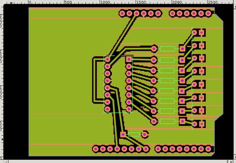
After downloading, open the files together in the viewer application and give them one last intense inspection. Don't be alarmed if everything, including your text shows up backwards or upside-down. It's normal, as the screens have to be reversed for etching on the other side of the board. But do make sure everything looks as good as it did in Fritzing. This is where you may discover things missing if you used a custom or 3rd party part with broken graphics. In that case you will need to fix the part SVGs and try again.
3. UPLOAD TO THE FAB
Fritzing's Fab service only accepts Fritzing files. Just go to File->Save or File->Save As... (Fritzing versions prior to 0.7 must use File->Save As Shareable). Then go to our Fritzing Fab page and to fill out the order form and upload this file. If you don't have all the parts you need, now might be a good time to print out the Bill of Materials under File->Export->List of Parts and go shopping. After that, maybe turn off your computer, write somebody a postcard or go skateboarding while you wait for the postman to come.
4. ASSEMBLE YOUR BOARD
Soldering tips are beyond the scope of this document but NASA, Sparkfun and Tom Hammond (PDF) have some great tutorials.
5. PROFIT!
A. TAKE A PICTURE AND A SCREENSHOT - UPLOAD IT TO FRITZING.ORG's PROJECT ARCHIVE
B. AMAZE YOUR FRIENDS
C. FOOL YOUR ENEMIES
D. GO INTO BUSINESS SELLING WIDGETS
E. CHANGE THE WORLD OR YOUR LIVING ROOM
Thats it really.